# DE10 Lite
# Capstone project Coursera
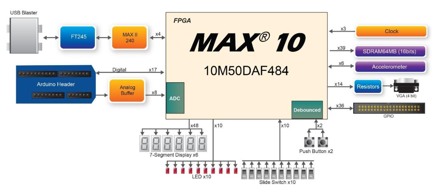
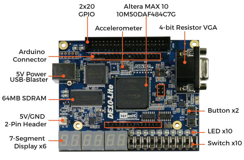
The DE10-Lite is an FPGA evaluation kit that is designed to get you started with using an FPGA. The DE10-Lite adopts Altera’s non-volatile MAX® 10 FPGA built on a 55-nm flash process. MAX 10 FPGAs enhance non-volatile integration by delivering advanced processing capabilities in a low-cost, instant-on, small-form-factor programmable logic device. The devices also include full-featured FPGA capabilities such as digital signal processing, analog functionality, Nios II embedded processor support, and memory controllers. The DE10-Lite includes a variety of peripherals connected to the FPGA device, such as 8MB SDRAM, accelerometer, digital-to-analog converter (DAC), temperature sensor, thermal resistor, photo-resistor, LEDs, pushbuttons and several different options for expansion connectivity.
# FPGA Device
• MAX 10 10M50DAF484C7G Device • Integrated dual ADCs, each ADC supports 1 dedicated analog input and 8 dual function pins • 50K programmable logic elements • 1,638 Kbits M9K Memory • 5,888 Kbits user flash memory • 144 18 × 18 Multiplier • 4 PLLs
# Memory Device
• 64MB SDRAM, x16 bits data bus
# Connectors
• 2x20 GPIO Header • Arduino Uno R3 Connector, including six ADC channels.
# Display
• 4-bit resistor-network DAC for VGA (With 15-pin high-density D-sub connector)
# Switches, Buttons and LEDs
• 10 LEDs • 10 Slide Switches • 2 Push Buttons with Debounced. • Six 7-Segments
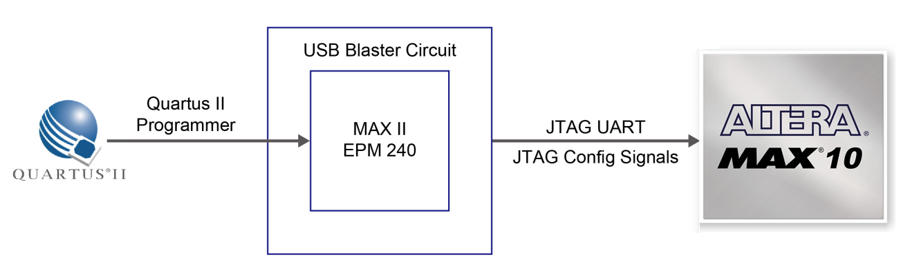
# Configuration of MAX 10 FPGA on DE10-Lite
There are two types of configuration methods supported by DE10-Lite:
JTAG configuration: configuration using JTAG ports. JTAG configuration scheme allows you to directly configure the device core through JTAG pins - TDI, TDO, TMS, and TCK pins. The Quartus II software automatically generates .sof files that are used for JTAG configuration with a download cable in the Quartus II software program.
Internal configuration: configuration using internal flash. Before internal configuration, you need to program the configuration data into the configuration flash memory (CFM) which provides non-volatile storage for the bit stream. The information is retained within CFM even if the DE10-Lite board is turned off. When the board is powered on, the configuration data in the CFM is automatically loaded into the MAX 10 FPGA.
# JTAG Chain on DE10-Lite Board
The FPGA device can be configured through the JTAG interface on the DE10-Lite board, but the JTAG chain must form a closed loop, which allows the Quartus II programmer to the detect FPGA device.
# Configure the FPGA in JTAG Mode
The following shows how the FPGA is programmed in JTAG mode step by step.
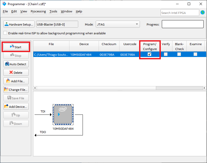
- Open the Quartus II programmer, please Choose Tools > Programmer. The Programmer window opens.
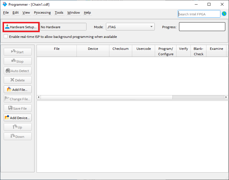
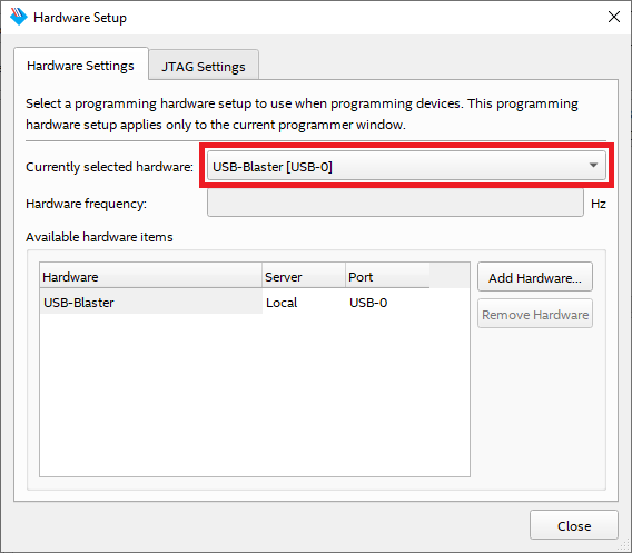
- Click “Hardware Setup”.
- If it is not already turned on, turn on the USB-Blaster [USB-0] option under the currently selected hardware and click “Close” to close the window.
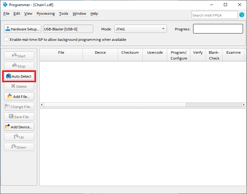
- Click “Auto Detect” to detect all the devices on the JTAG chain.
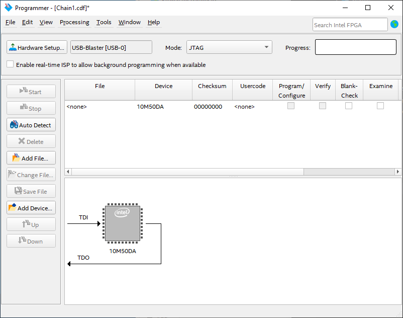
- Select the detected device associated with the board.

- FPGA is detected.
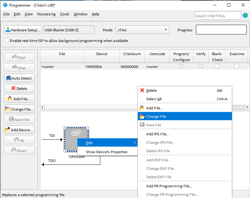
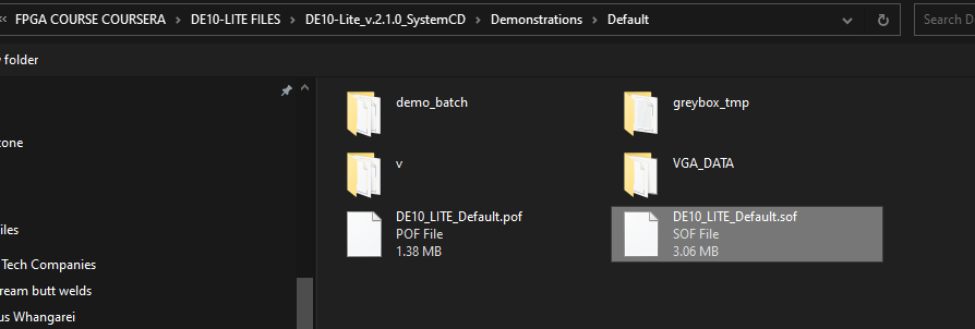
- Right-click on the FPGA device and click “Change File” to open the .sof file to be programmed.
- Select the .sof file to be programmed.
- Click the “Program/Configure” check box and then click the “Start” button to download the .sof file into the FPGA device.
# General Design Flow - Quartus
This section provides an introduction to the design flow of building a Quartus II project for DE10-Lite under the DE10-Lite System Builder. The design flow is illustrated in Figure 4-1.
The DE10-Lite System Builder will generate two major files, a top-level design file (.v) and a Quartus II setting file (.qsf) after users launch the DE10-Lite System Builder and create a new project according to their design requirements.
The top-level design file contains a top-level Verilog HDL wrapper for users to add their own design/logic. The Quartus II setting file contains information such as FPGA device type, top-level pin assignment, and the I/O standard for each user-defined I/O pin.
Finally, the Quartus II programmer is used to download the .sof file to the development board via the JTAG
interface.
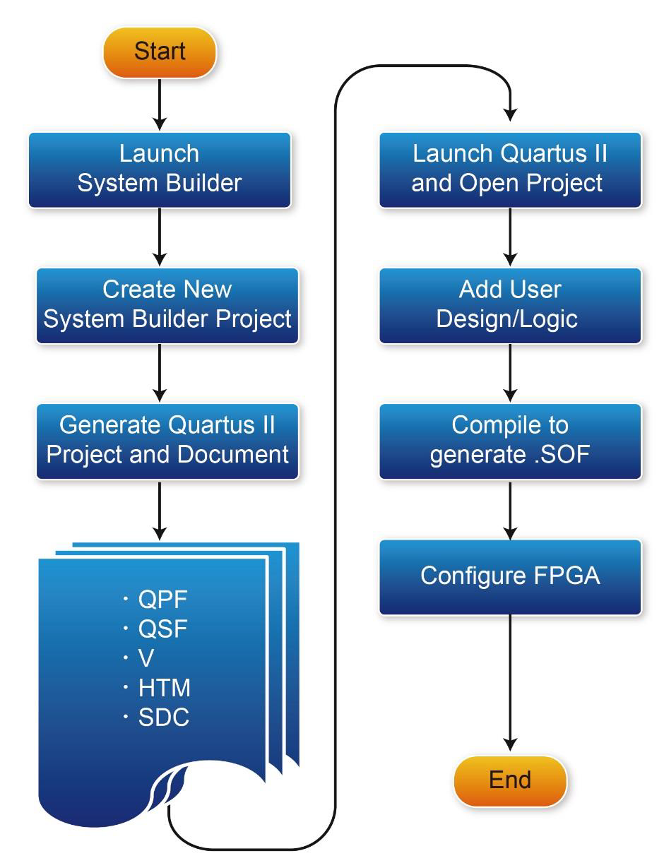
Using DE10-Lite System Builder, see DE10Lite manual page 44.
# NUMBERS AND DISPLAYS
This is an exercise in designing combinational circuits that can perform binary-to-decimal number conversions and binary-coded-decimal (BCD) addition [1].
# PART I – DISPLAY SWITCH VALUES

We wish to display on the 7-segment displays HEX1 and HEX0 the values set by the switches SW7-0. Let the values denoted by SW7-4 and SW3-0 be displayed on HEX1 and HEX0, respectively. Your circuit should be able to display the digits from 0 to 9 and should treat the valuations 1010 to 1111 as don’t care.
module SEG7_LUT	(	oSEG,iDIG	);
input	[3:0]	iDIG;
output	[6:0]	oSEG;
reg		[6:0]	oSEG;

always @(iDIG)
begin
		case(iDIG)
		4'h1: 	oSEG = 7'b1111001;
		4'h2: 	oSEG = 7'b0100100;
		4'h3: 	oSEG = 7'b0110000;
		4'h4: 	oSEG = 7'b0011001;
		4'h5: 	oSEG = 7'b0010010;
		4'h6: 	oSEG = 7'b0000010;
		4'h7: 	oSEG = 7'b1111000;
		4'h8: 	oSEG = 7'b0000000;
		4'h9: 	oSEG = 7'b0011000;
		default:	oSEG = 7'b1111111;

		endcase
end

endmodule
2
3
4
5
6
7
8
9
10
11
12
13
14
15
16
17
18
19
20
21
22
23
24
SEG7_LUT Verilog fileStructural coding is to be inserted at the end of the DE10_LITE_Golden_Top.v file.
...

//=======================================================
//  REG/WIRE declarations
//=======================================================


//=======================================================
//  Structural coding
//=======================================================


assign LEDR[9:0] = SW[9:0];  // led is high active


assign HEX5 = 8'b11111111; // low active
assign HEX4 = 8'b11111111; // low active
assign HEX3 = 8'b11111111; // low active
assign HEX2 = 8'b11111111; // low active
assign HEX1[7] = 1'b1; // low active
assign HEX0[7] = 1'b1; // low active


SEG7_LUT	SEG7_LUT_v_2 (
	.oSEG(HEX1),
	.iDIG(SW[7:4])
);


SEG7_LUT	SEG7_LUT_v_3 (
	.oSEG(HEX0),
	.iDIG(SW[3:0])
);


endmodule
2
3
4
5
6
7
8
9
10
11
12
13
14
15
16
17
18
19
20
21
22
23
24
25
26
27
28
29
30
31
32
33
34
35
36
37
38
39