# Altium Designer
# 1. User interface
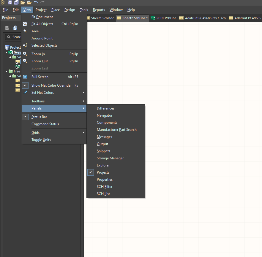
To call panels use the View-->Panels menu:
TIP
Library Panel is now Components Panel
TIP
View Controls:
Pan - right click Zoom - middle button pressed up and down - scroll
System preferences are in Tools-->Prferences
# 2. Schematic Design
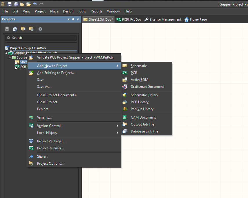
# Creating a new project
File-->New-->Project-->PCB Project
To add new documents, right click on the project and -->New to Prohect, and choose.
Now most likely you'd like to save all these files out and maybe give them more appropriate names, so to do this I can just again right-click on the project, choose Save Project As, and this will actually ask me to save out anything that has not yet been saved, so the top level PCB Project file as well as each of the Schematic sheets, each of the PCB layouts, really all the files within that project.
# Installing and using libraries in Altium
At the components library, let's take a look at miscellaneous devices here. And what I have here is just a whole number of different components and I can navigate through these here and I get a nice visual preview of the schematic representation as well as the PCB footprint of that specific component. Now of course you can customize and create your own libraries as well and we'll dive into that a little bit later on in this course, but you can also install, use, and download a whole number of already existing libraries. So let's take a look at installing a simple library here.
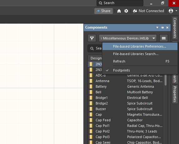
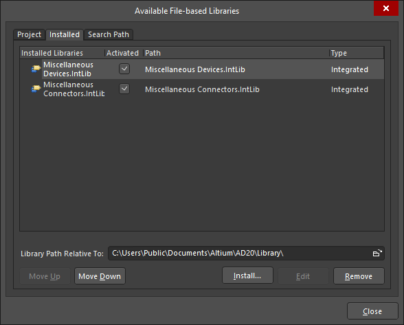
Here you just click install and choose the existing library.
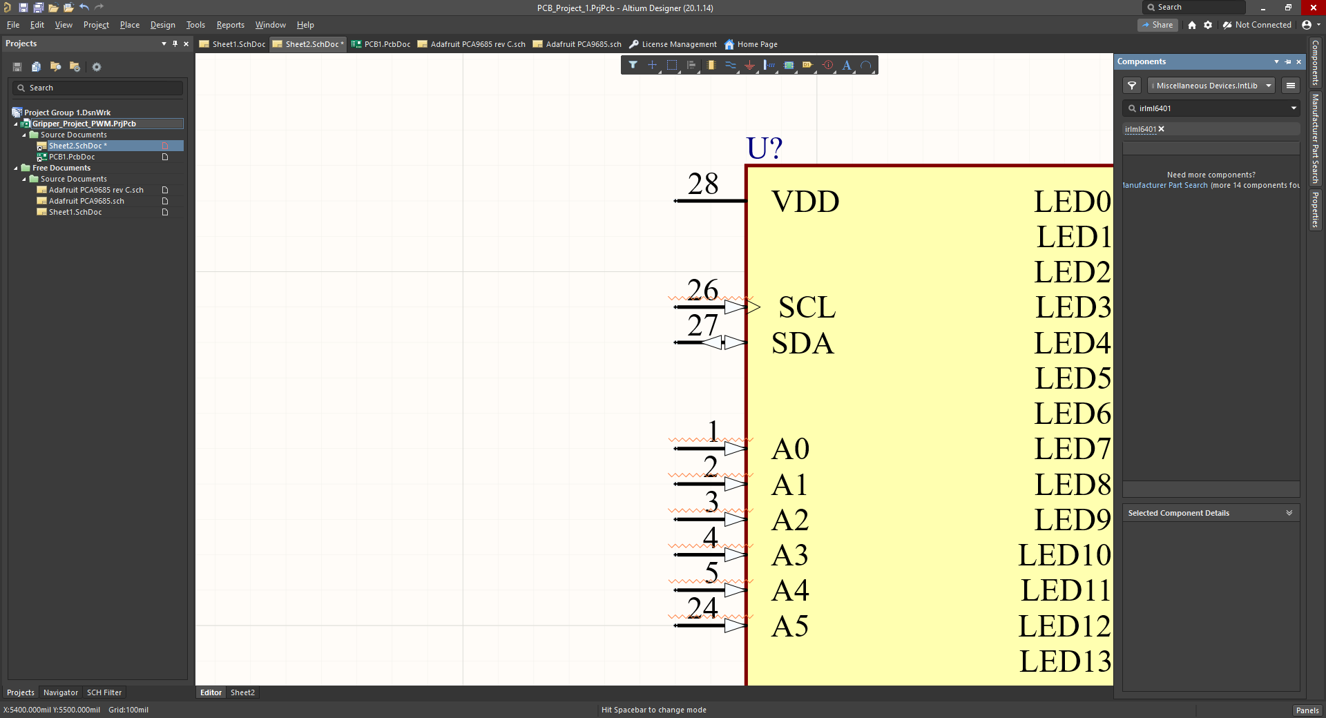
# Placing component in schematics
Within the library of choice you can drag and drop the component or right click and place component.
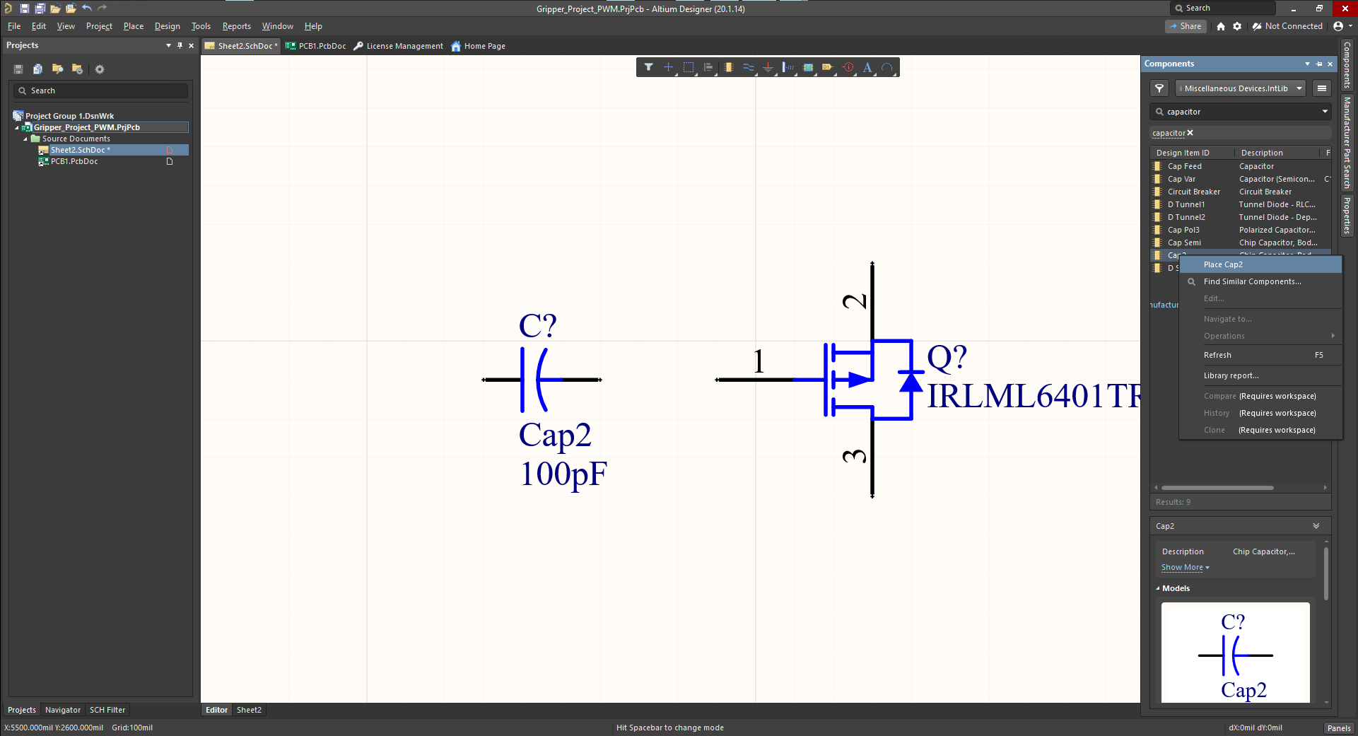
One benefit of using the right-click and place component is that I can place multiple components here and not have to do click and drag multiple times.
In addition to this, I do have a couple of other capabilities while inserting. I have a few hot keys I can use here. I can use the space bar, which as you can see, will rotate my components 90 degrees.
Also, if I hit the x key, that will flip my component orientation about the x axis. And similarly, if I hit the y key, it will flip the component in the y axis.
Press esc to scape.
One further option in placing components is just to double click and that will essentially be the exact same as my right-click place component option, and it's just going to bring in and I can now click to place as many components as I may need.
# Component properties and inserting ports
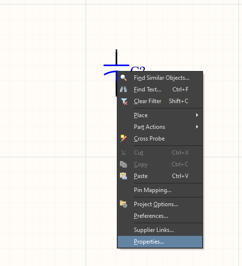
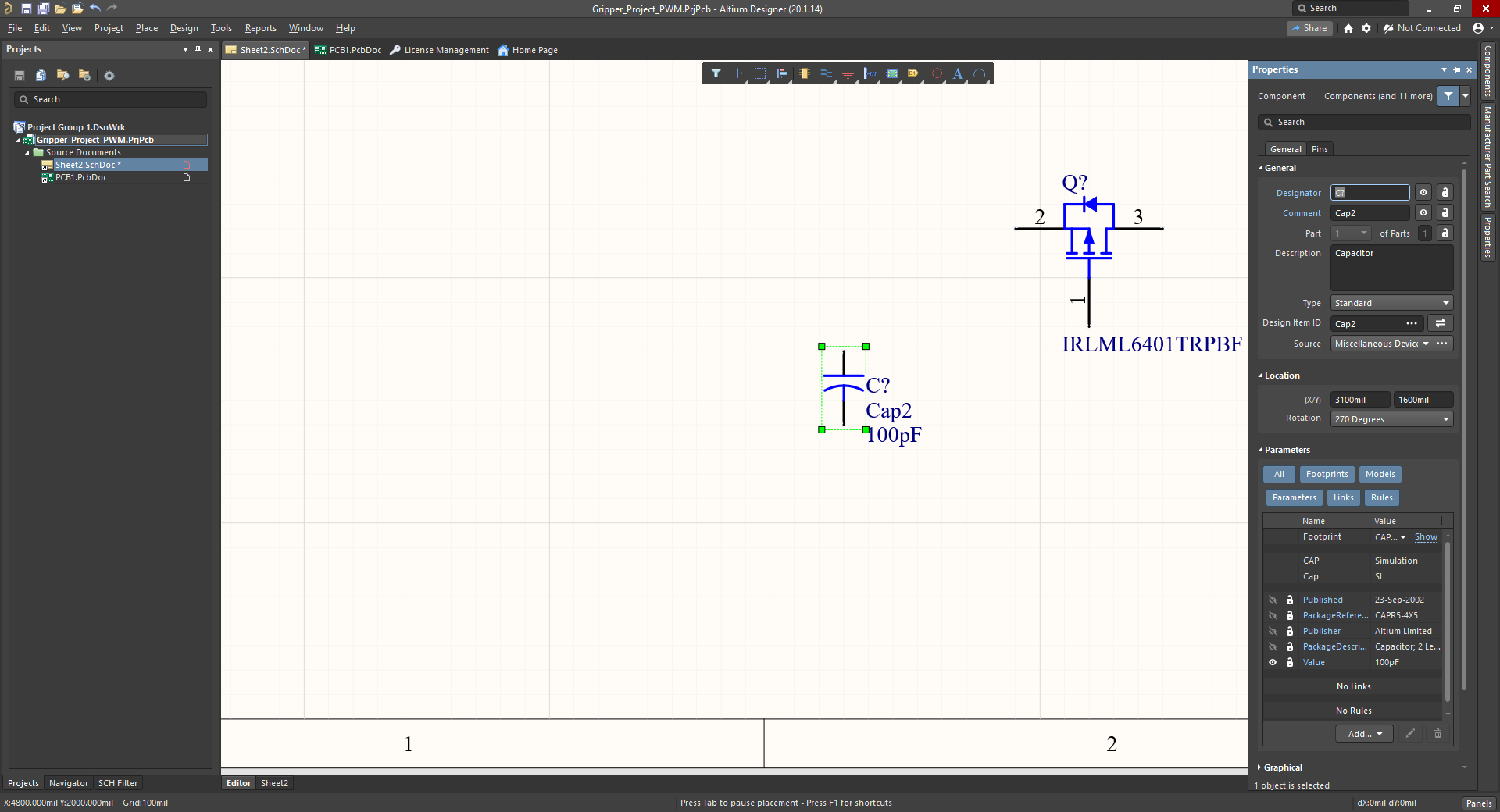
Just right click on the component and go to properties to open the properties side panel.
That should open my Properties side panel here and as you can see, I have a whole number of properties. I can change the description, the designator, type, location, and so on. Can also navigate to creating some custom parameters for the properties I may need there. And I can even add or customize the specific Pin values and the specific Pin properties for each component, as well.
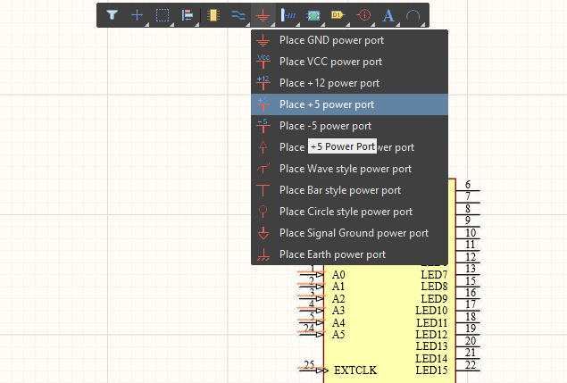
To insert power ports, I can just navigate up to my active bar here. I have a lot of commands here. Right in the middle here, I'm seeing some of my power ports and I'm seeing actually a ground power port so that's something I'm probably going to use quite often, insert a lot of ground symbols. So I can just click on the ground and place my grounds wherever I'd like.

Now I do have a number of additional power port options, as well. I can just click and hold for one second on the active bar here and it's going to show you all the other options so maybe I want to place a few VCC power ports, as well here and I can just place a few of these ports, as well. With the power ports I have that same option. To navigate to the properties, just do a double click, a right click on properties, or right as I'm placing, I can just hit the tab key and that's kind of a hot key to jump right into the properties as I'm actually placing these power ports here.
# Wiring the schematic
To start wiring our schematic, I can just navigate up to the active bar and this icon in the middle here has a number of wiring options for me. So, just to start, we can use Wire. And now it's a very simple process, just click once to start our Wire and click again to finish our Wire. Also notice, if I hover over any pins or electrical connection points, I should see my X getting a little bit larger and turning red. So, that's just indicating to me that right on this pin 17, there is an electrical connection point that I will connect to.
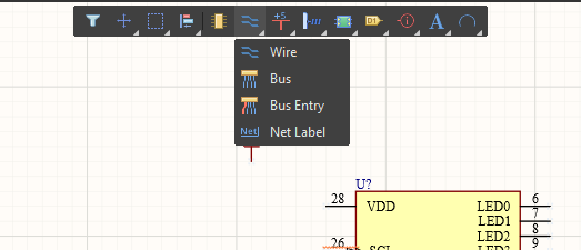
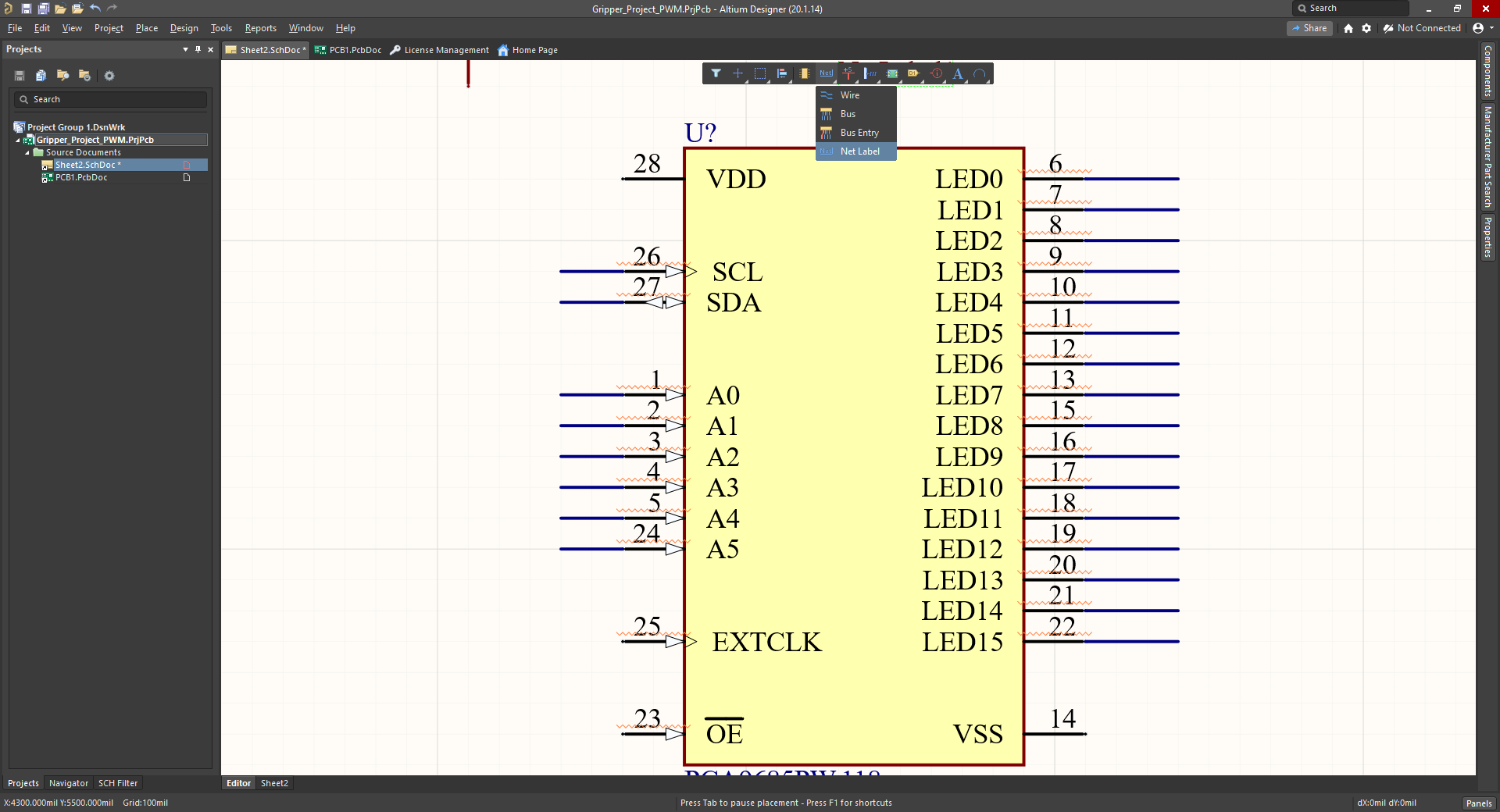
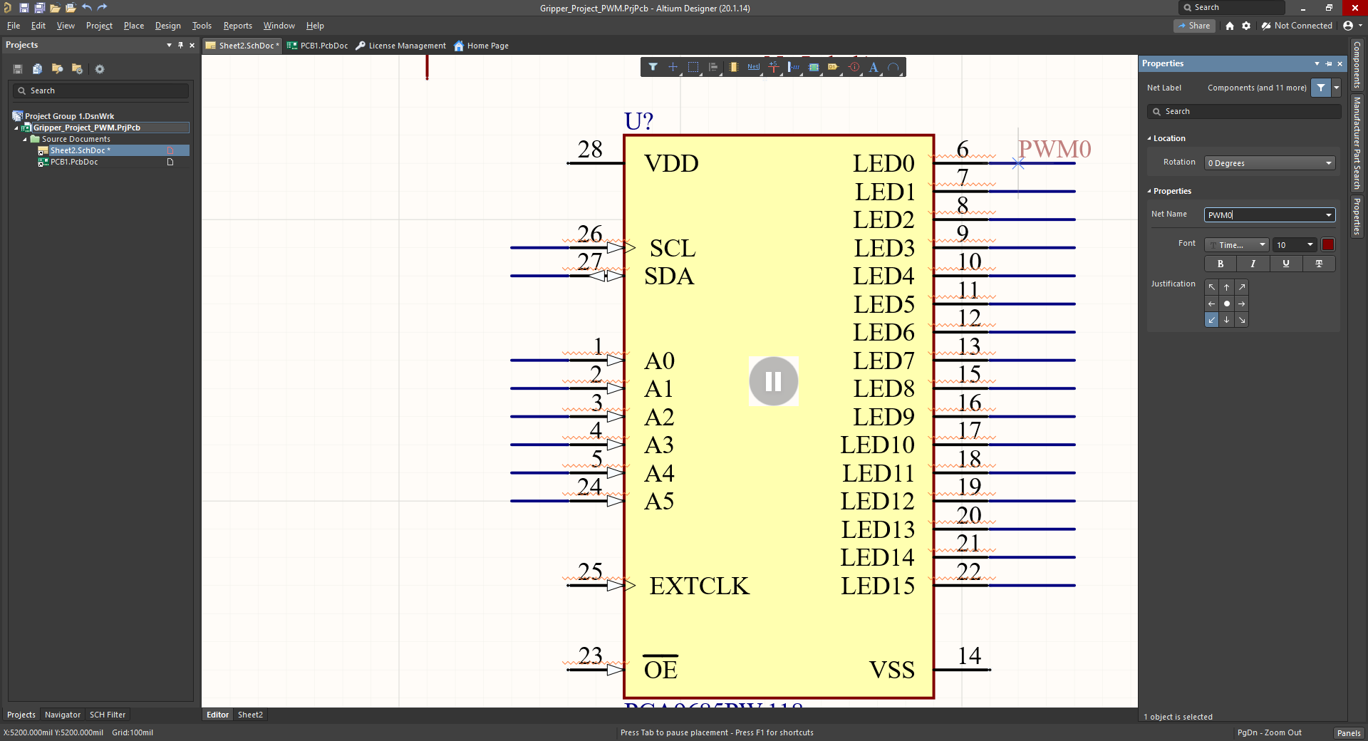
One other important aspect to make note of is using the Net Labels. So, again, if I go over to my Wire command here, and I have an option for Net Labels here. So, Net Labels can be very useful to give a specific label or connection point to any wires or name essentially, and this can really help simplify drawings. So, what I can do with this is actually make electrical connection points just within that label and then I don't actually need a physical connection. So, let's take a look at that. First, I have the default name here in that label. If I hit Tab again, I'll jump in to those properties, and I can change to maybe a more suitable name here, and this one I'll call Swire at D9 and the next will be D10. Notice, that automatically it jumps to the next numerical value , or of course, you can change the name manually just in the same way with the properties there.
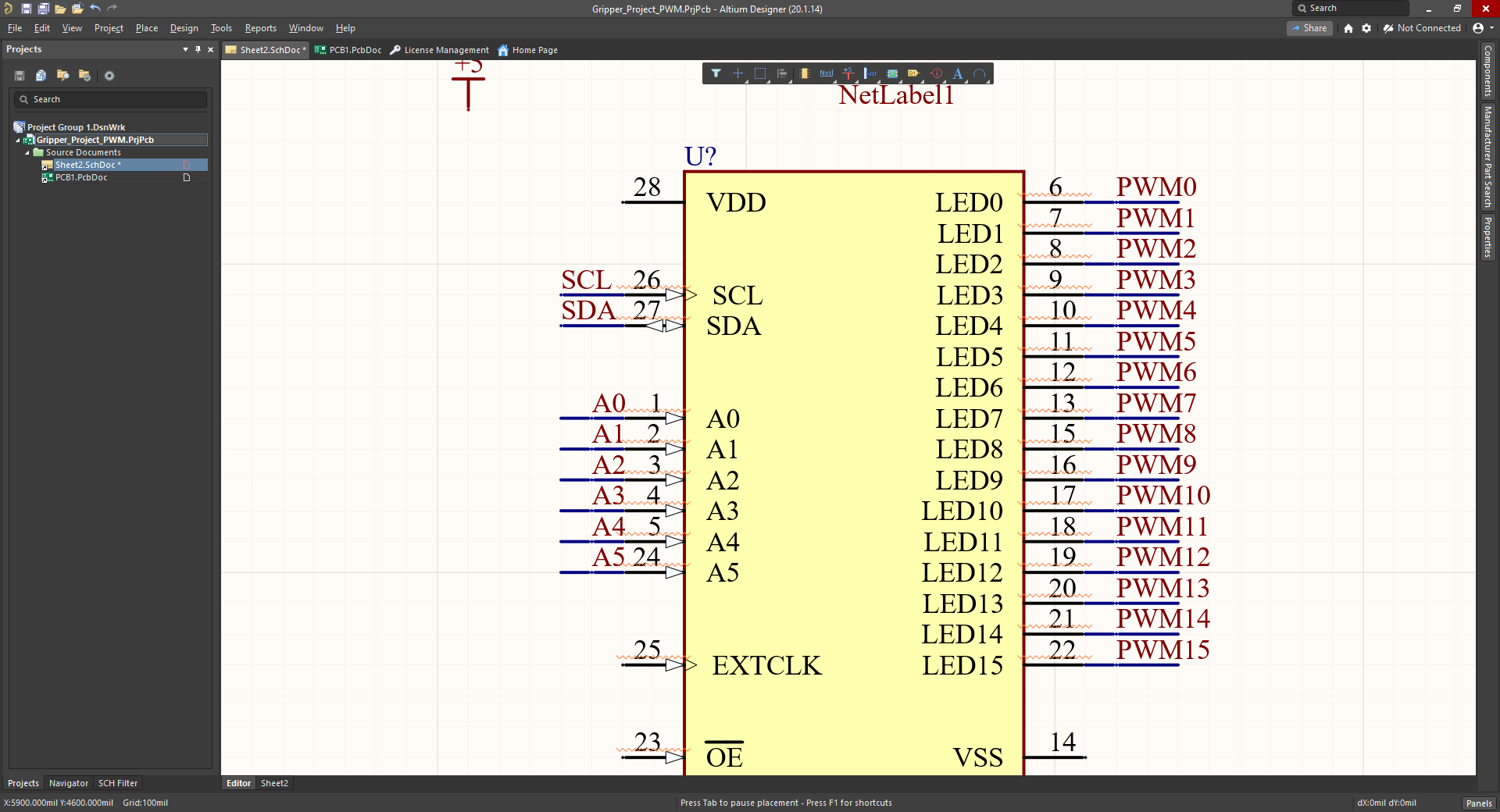
Okay, so let's throw in some Net Labels like this here and then the idea is here, I can actually make connections that aren't necessarily physical connections. So, let's say I want to connect D12 and D13 here over to the other side of my Schematic, and I don't want to cross over a bunch of existing schematic wires and components and so forth. So, what I can do is draw a few more wires over my components here and then just add those same corresponding Net Labels. So, add a net label here and now let's call this not D14 but let's change that to say, D12 and D13. And just hit Escape to finish off there.
# Annotate schematics
A very useful tool in Altium Designer is the ability to automatically annotate your schematic. So, as we briefly saw earlier, one way I can annotate my schematics and my component is just by doing this manually. So, again, I'll just go into any components properties, so I can do that with a double click, here, and just change the designator names of each and every component one by one, here. Right, and that would be annotating my schematics in a more manual method.
However, I also have the ability to do this in a much more automated way. So, another option I have is I can just navigate up to the tools--> annotation--> annotate schematics.
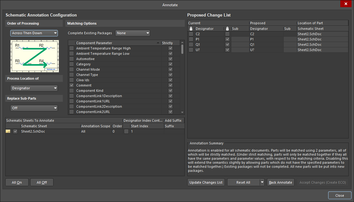
So, here is maybe a much quicker way to annotate all of your components within your schematic, so here, we see all of the current components that I haven't yet given a unique designator, and, so it's just going to go through each of these and try to automatically annotate them, and it does this based on a number of things, one of them being the order of processing. So, I can change this depending on my specific standards, but currently, it's going to number them in order of across and then down, as we kind of see with this visual, here, and I have a few other options that I can choose from based on my own numbering systems. In this case, I'm going to use, you know, one of the most commonly used ones, which is across then down.
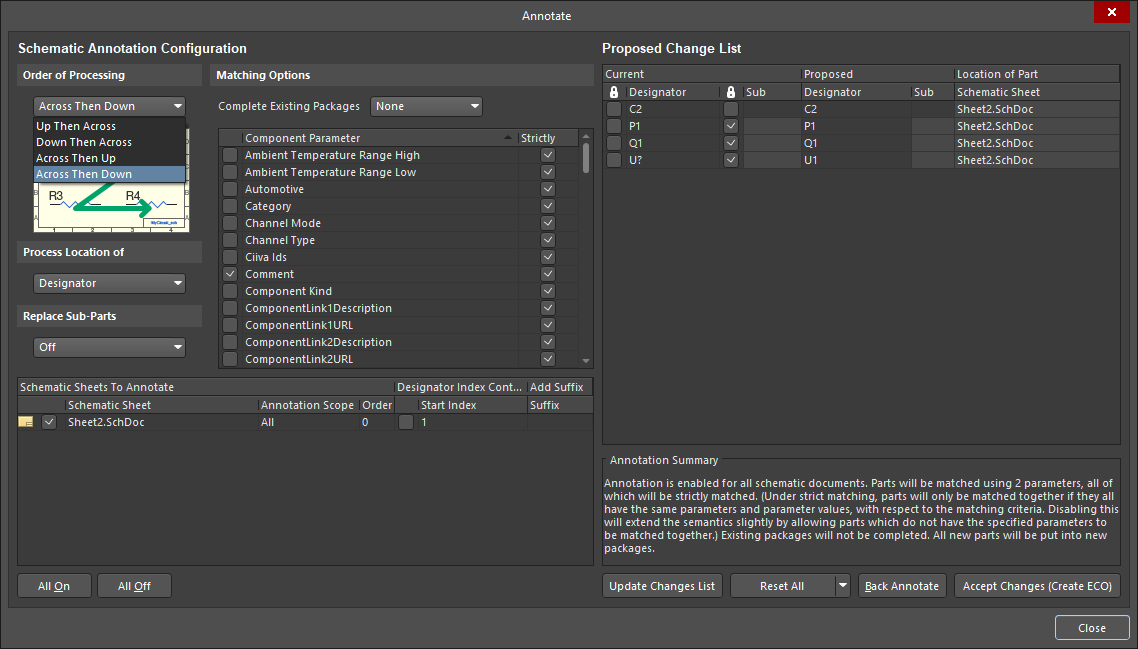
and I can also manually override this, here, I can change the designators manually, here, as well, or if I want to try to automate that process a little bit further, I can just go to update, change this list here, and here, it's telling me, so, right now, I have 33 components, that don't have a unique designator, so it's going to make 33 changes for me. So, I can say okay, and what's nice, it actually shows me the current designators, here. All the question marks, 'cause they haven't been correctly identified with numbers, and then the proposed changes, so how the numbering's going to come in. Again, you can override this manually if needed, of course, but once you're happy with this, the next step I can go it to accept my changes.
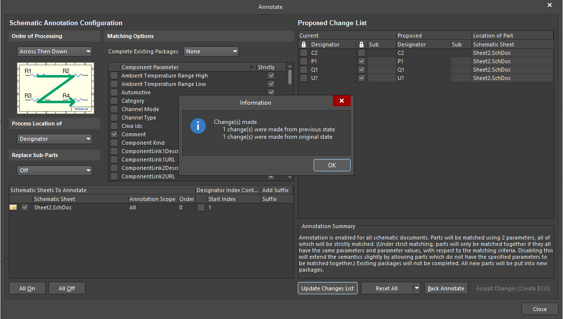
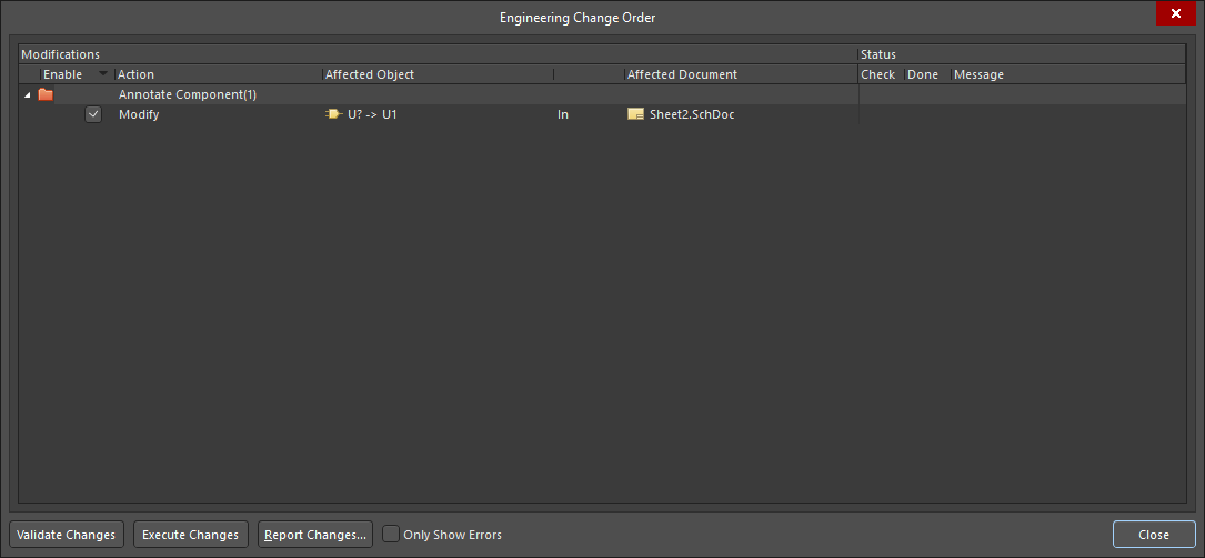
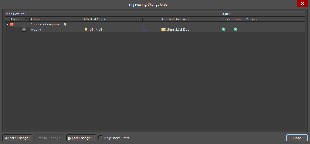
So, I'll just click accept changes, here, and this will jump me into my engineering change order. So, essentially, it's going to show, individually, all of the modifications or changes that will be automatically occurring, and I can agree to these or disagree to these, modify them as needed, but let's say I'm happy with all of these for now, then I can just click on validate changes. Okay, so it will check if all of the changes can be validated and if they can, I'm going to see a number of green checks, here, giving me the green light, and once I'm happy with that, I can then just click on execute changes to actually execute all of these changes within my schematics. Again, seeing all the green checks giving me the green light that this has now been completed, and I can just close out of this, and close out of this, as well, and now I can take a look at my schematic and I should see that all of my component designators, now, have been changed to unique designators. So, it used to be C question mark, C question mark, C question mark, and so on, 'cause I didn't give them any specific names or designators, and now they've all been named and numbered in order as the across and down.
# Compiling an Altium project
Compiling an Altium project is a critical step to check or test if there may be any potential issues or errors within your design. So generally this is something you might do later on in your design, or for sure when you're finished your design, just to double-check to see if there might be any problems within it.
And it's, again, a very simple process. I can just navigate over to the Project dropdown here. And right at the top I have the Compile option (Validate Project Option).
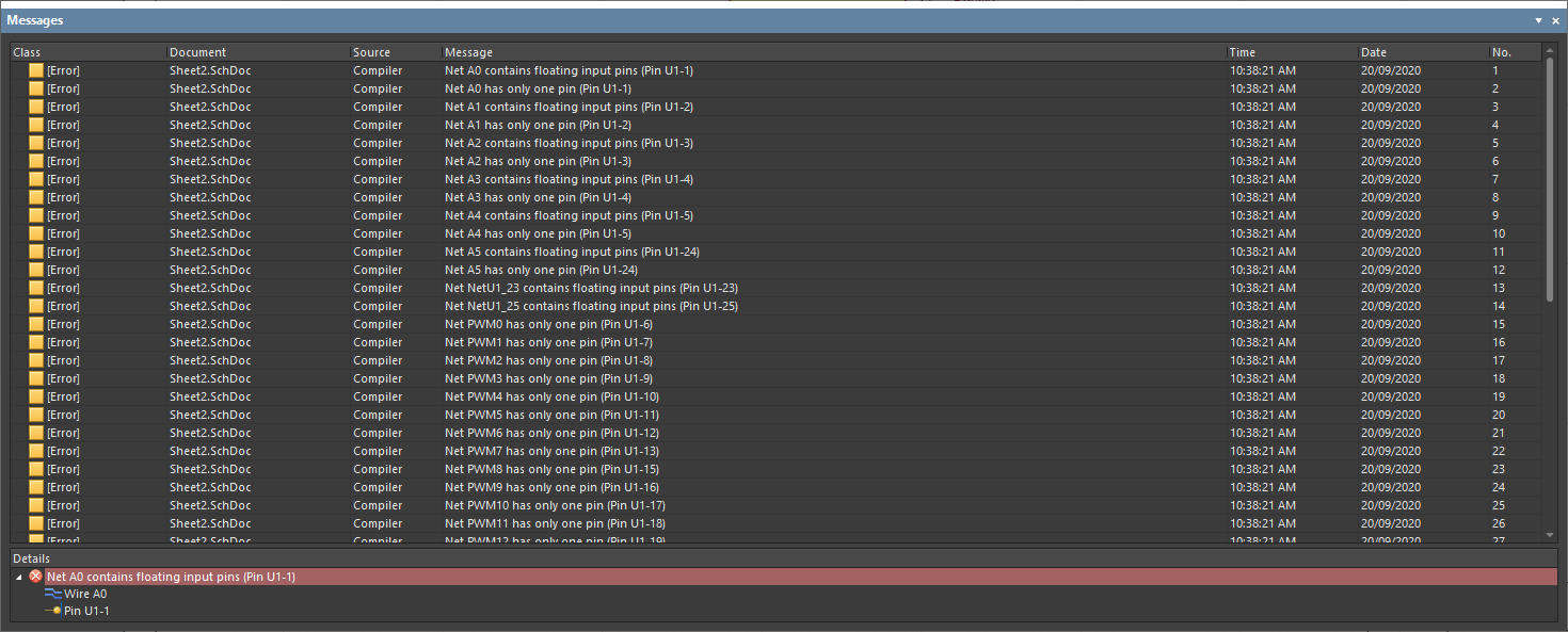
If I've made all the necessary fixes to those errors and warnings, now I'm just seeing that I have a completed Compile here.
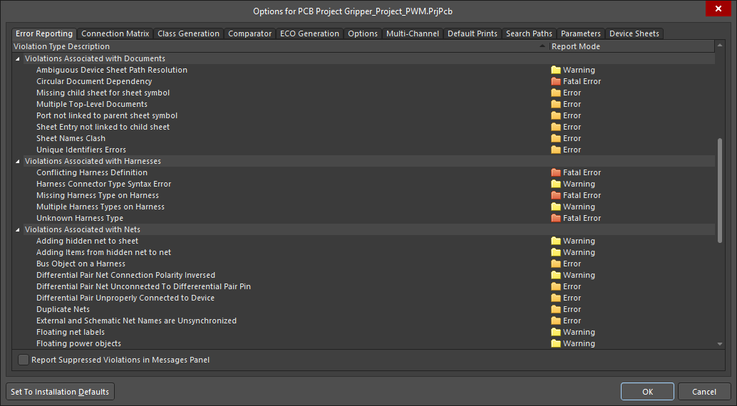
So, one question we also have to ask ourselves here is where, exactly, are those rules coming from that we're testing against. And those can be completely customized. So, to customize those rules, again, I just navigate to the Project dropdown and all the way down at the bottom I have Project Options. And here are my error reporting options. So these you can completely customize and change to fit your own specific needs for your specific projects. And for any of these violations, I can change to, maybe it's just a warning, maybe it's an error or a fatal error, or maybe it's no error at all, depending on what we need for our projects.

# PCB Design
# Layer Stack Manager
To get started I'll want to set up my settings, and my options.
So one option I can manage is just by going up to the Design-->Layer Stack Manager. And most likely you'll only want to set this up once, or twice and you can save these out actually as templates, so you don't have to redo this every time you starting a new project. But here we can add, remove, change, however we may like to our layers within our boards.
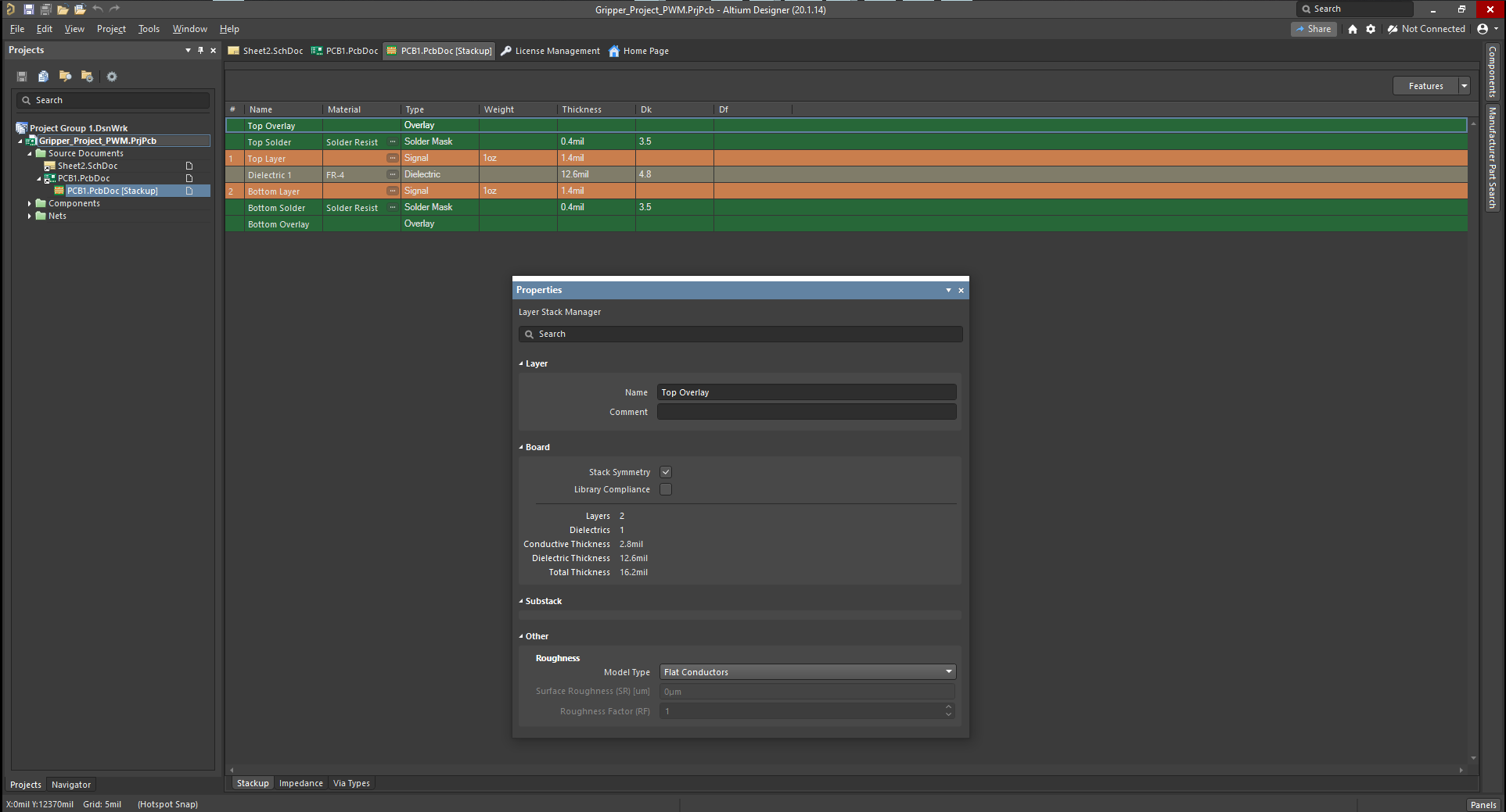
So here's just kind of the Altium Designer default here. You can see I have two signal layers. And I can change any of the values here. And so I can just double click on any of these values and make edits and changes as I may need. And I can also add and remove layers, so if I add a layer here, let's add one more Signal Layer, and now I'm seeing a new Signal Layer coming in here. And of course I could delete that layer as well. So in this case we only want the simple example, the two layers here, but you can see you can completely customize your Layer Stack Manager to your own needs. And then once I'm happy with all of that I of course can save this out, if I'd like to use it again, I can load old settings as well. Or just say OK once I'm happy.
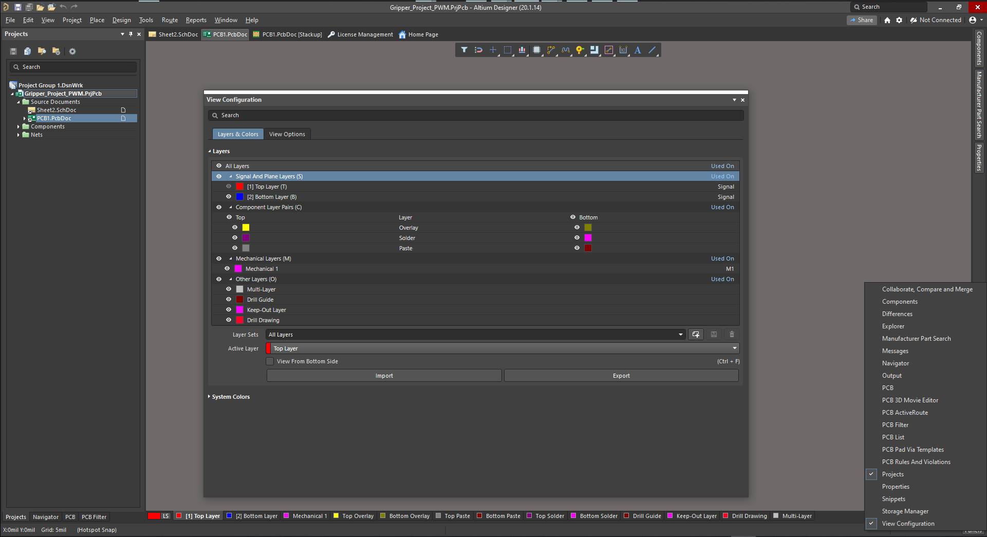
Another useful settings or options for your PCBs is the View Configurator. So I can just double click on this Current Layer icon down here. And that should pop up a new window for me as well, called the View Configuration. Alternatively, I could go into my panels, and turn on my View Configuration on or off here. So here we have all of our layers described to us, and the colors being showns. Right now I just have the two Signal Layers, top and bottom. And once I start placing components and routing some traces there they'll come in as the red and the blue I can see. But I can change these values, these colors if I'd like to really any color I would like for any layer I would like. And that's just to help you visualize your PCB designs. In addition to this very use-ful I can add or use mechanical layers here. So right now I just have a Mechanical Layer one, but if I'd like I can just right click Add additional Mechanical Layers. Switch which Mechanical Layer I'd like to throw it on, so currently I have one on M one here, maybe I want to use another M two, let's say. And now I have Mechanical one and Mechanical Two Layers. So I can add in a whole number of mechanical layers and these you can just be used to help with your design process as well, and I can edit, or change these names if I'd like, so let's maybe edit this layer, and call this Dimensions or something like that. So you can add as many mechanical layers as you'd like, rename them, so now maybe I'll just add in some board dimensions on a mechanical layer. And then once I'm happy with that I can close out of this as well.
So really these two options are just to help setup the background options and settings of your board design before you get started with your PCB layout design.
# Grids and units
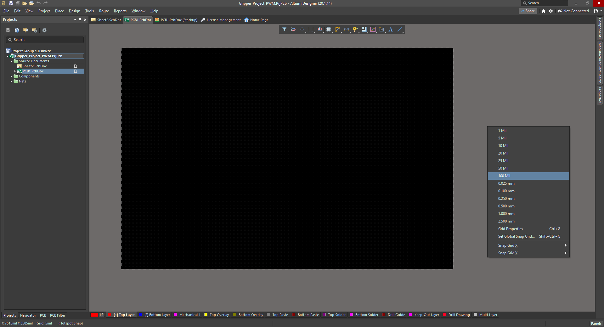
So, one of the first things you'll want to set up correctly when starting off your PCB Board designs is to make sure that your units and your grids are correctly set up for your project. So let's take a look at this project initially. Doesn't look like there's even any grid at all. Actually, if I zoom in a little bit here, I can see that, in fact, there is a grid with some dots and some lines here as I zoom in further and further. So the reasoning behind that is just that my grid is fairly small, compared to my entire board size here. If I want to change that really quickly, I can just hit the G key for grid and I can change my grid size. I believe right now it's at five millimeter. I want to change that to 100 mill so the grid size will be a little bit larger and between grid steps will be larger.

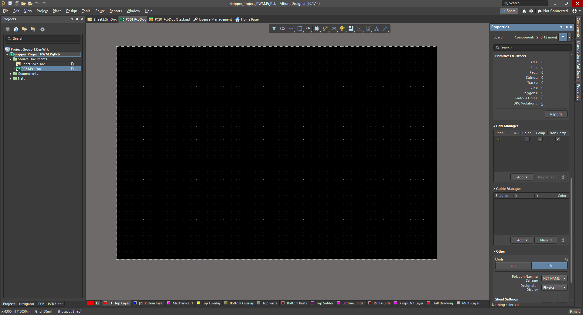
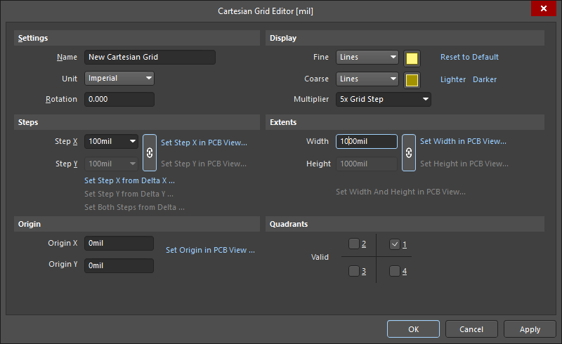
Let's say I want to customize my grids a little bit further. This is just the global grid. I can customize my grid by going into Properties. Let's check my panels here. Go into Properties, and this is when I'm within my PCB Board design. And scrolling down, I have a bunch of options here. Object snapping, board size. And down here, I'm seeing Grid Manager, so I just have the one grid here and that's my global grid but if I'd like to create some custom grids, I can do that as well. So I can just choose Add and I have the option of Cartesian Grids or Polar Grids. So let's start just with a simple Cartesian Grid and then I can double-click on that Cartesian Grid to jump into the Properties or Options of that a little bit. And then I can customize the units here, the origin, the steps, let's say, 100 mill by 100 mill. Maybe the color just so we can see the differences here. And so on, the total extents. Let's see, maybe 1,000 mill. Okay, and which quadrants it's coming in here. So I'll just change some quick settings there, say Apply and OK.
So I should now see a new Cartesian grid coming in. Starting from my global origin point, but I could re-figure that origin point as well. The total size and the grid spacing I chose there. So Cartesian grid, fairly simple.
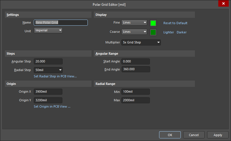
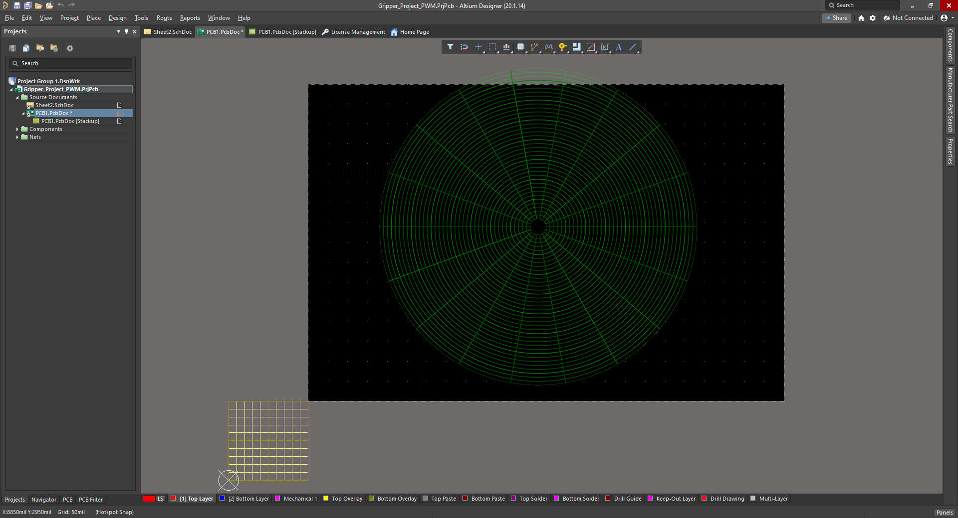
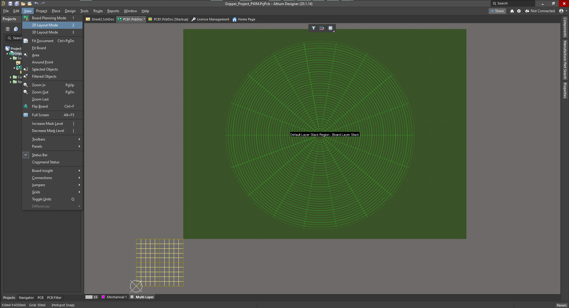
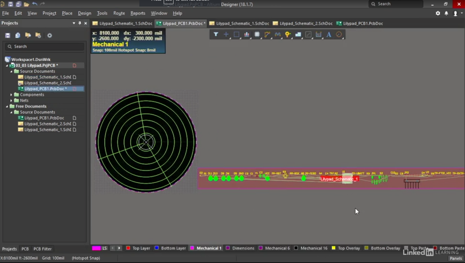
Let's say I want to create a polar grid as well, because my lily pad board design is actually a circular board, so it might be also helpful to have a circular grid to help me place components and so on. So, there I would, again, go to Add, but this time choose Polar Grid. And again, I'll double-click on my polar grid here. And I'm going to change some of those properties as well. So, set the units. Set the angular step and the radial step. Maybe my angular step to be 20 mill. Radial step, maybe 50 mill or so. And then here, maybe I want a different origin. I can actually set my origin within my PCB view. So let's try this and just click wherever I'd like the origin of my polar grid to start. Let's say, right in the middle here, for example. And then, if I'm happy with that, again, I can say Apply and OK just to take a look here. And we can start to see my polar grid coming in. Not exactly as I'd like here, so let's customize this further. So I'll just double click on that polar grid again here. Just to make it more visible, I'll change the colors again here. Let's change it to green. And I actually want it to go 360 degrees, not just 90 degrees. So I'll change the start angle to zero and end angle to 360, so it should go all the way around. The origin point is okay, I've set that myself. The steps, I believe are okay. And then the radial range. It seems a little bit smaller right now from my lily pad board shape. I know it's about four inches, three or four inches, so maybe I'll change my radial range to say, let's say, the radius would be about 2,000 mill. And hit Apply and OK to that.
And now I can see my polar grid coming in a little bit stronger here with the green color. And the total size would be about four inches or so there.
So this is just a quick introduction to how you could set up, not only your global grid, change properties to your global grid, but you could also create as many custom grids as you may need to fit your own specific project needs.
# Board shape
We have a number of different methods to set up or change our board shape. So the first one we can take a look at is just go to my View drop-down and I would get to Board Planning Mode.
And next go into Design and here I can redefine my board shape, Edit or Modify Board Shape, Move and so on.
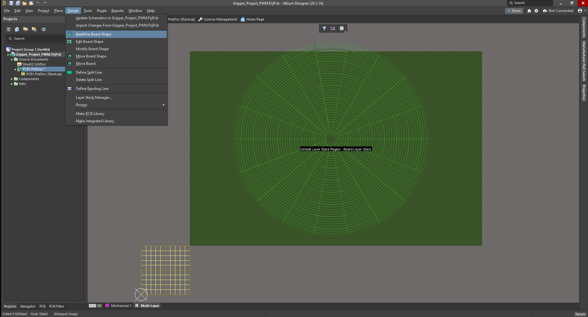
So let's try Redefine Board Shape, it's probably one of the simplest methods. And then I can just click to sketch out or regenerate really any board shape I like. So let's do something like this. I'm just making my board shape just a little bit larger here as an example. Yes and I've redefined this board shape just to be a larger rectangular board as an example. And if I'm happy with that, I can go back into my View and back into my standard 2D Layout Mode view.
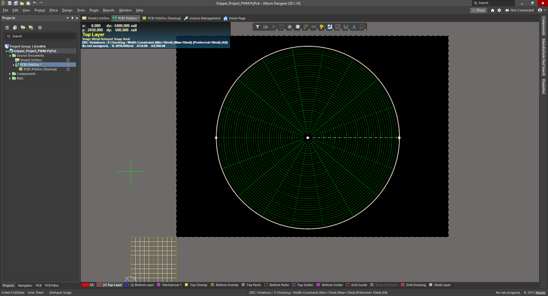
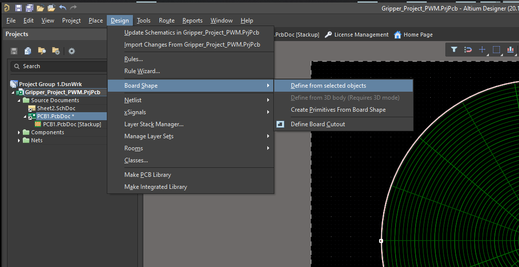
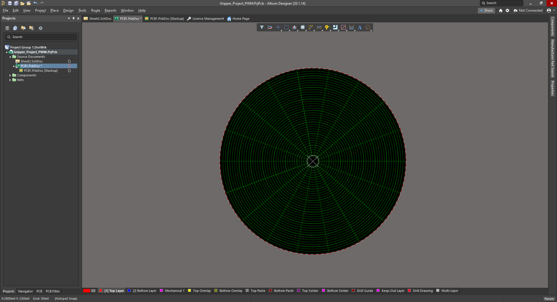
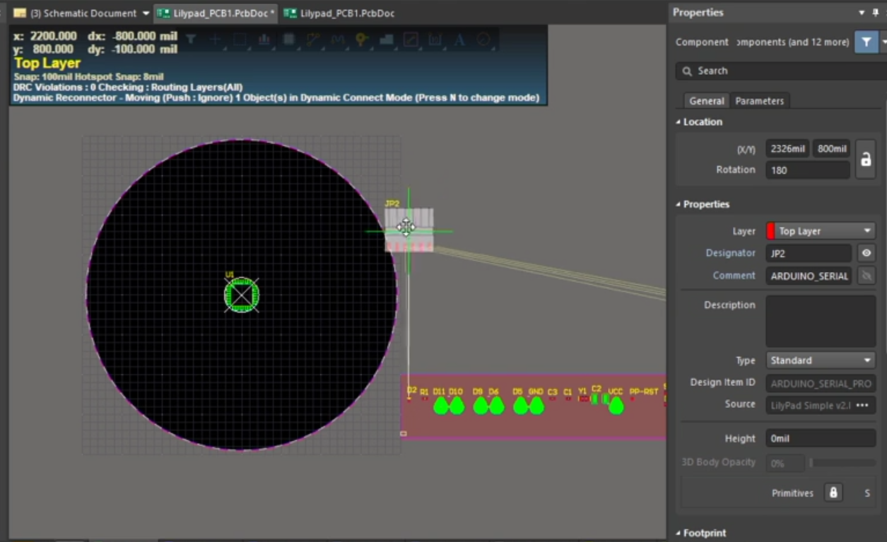
if I'm happy with that, I can go back into my View and back into my standard 2D Layout Mode view. And now I have a larger PCB board. I have a number of more complex options as well. Let's say for the lily pad again, I want it to be a circular board. So one option I have if I just go to Design Board Shape, I can really create a board shape from a number of other different methods as well. I can create from a 3D body if I have a 3D body or I can see here I can define from any selected objects so essentially any sketch or drawing within my workspace here, I can generate a board from. So in this case, what would make sense is just sketch out a circle, draw out a circle. So I can go to my drawing commands here and I can do lines, arcs, full circles, and so on so I can really create any kind of more complicated shape but I'm just going to start with a full circle. And say I'm going to want to start it right in the middle of my polar grid that I've created there. And I'm just really drawing a circle on really any layer, I'm using a mechanical layer here. But I want it to be again, let's say, something about this. So about that 2 inch radius or so.
So now that I've drawn out that circle on my layer here I can use that circle to generate my board shape so now I can just go back to the Design Board Shape and say Define from my selected object, so define from that circle that I'm currently selected on, and now you can see I have a nice circular board shape with my polar origin which might be helpful for placing components on this circular board later on.
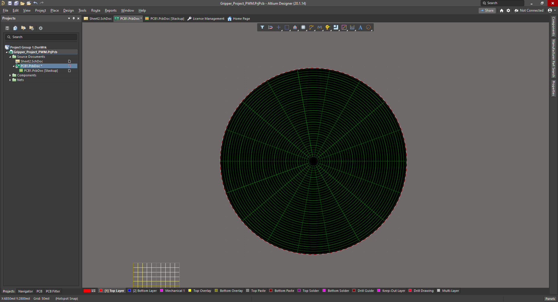
origin which might be helpful for placing components on this circular board later on. I want to just hint is my origin here is still the default or global origin. I can change this as well if I'd like. So maybe I want to put it at the center of my board. So I'm just going to go to the Edit drop-down and I have Origin and I have Set and Reset.
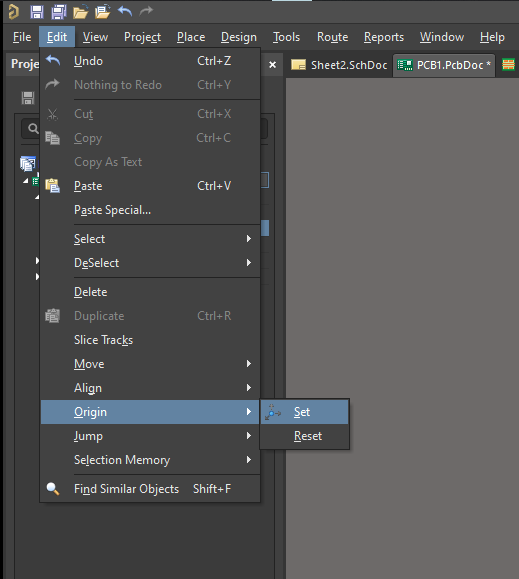
So let's say I want to set it here. Just place anywhere I'd like to set, in this case let's say, dead center my PCB here. And now there's my new origin so we can see as I move along the origin, the values are changing here. So I can be more specific with my component placements. If I want to jump back to the global origin, of course, just again, Edit, Origin, and Reset will get me back to my global.
# Pushing footprints from schematic to PCB
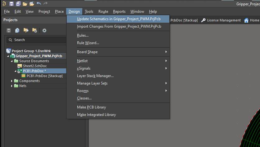
If we have already finished off our schematic design, as we have in this case, it's a very simple process to then just push over all of those electrical components into our PCB layout design. So, for example, I have my schematic that we've already created here, with all of the electrical components placed. And now I really just want to push those over to the PCB layout, eventually then we'll do the placements and the routing and so on. So we have two options here, we can do this from the schematic side of things or the PCB layout side of things and it's a very similar idea. Just navigate over to the design dropdown and if I choose update PCB here, that will push all of the electrical components over to my PCB layout.
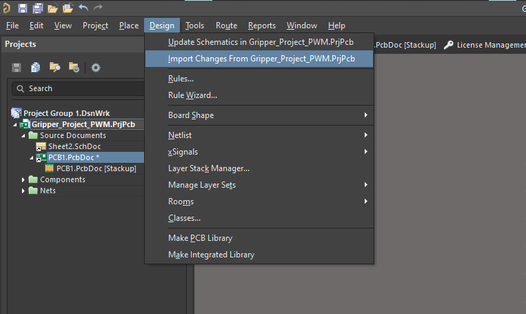
Alternatively, from the PCB layout file, very similar idea, just navigate, again, to that design dropdown and choose import changes, which will, again, push all those components over to my PCB layout.
So let's try this from the PCB layout side, I'll say import changes. And what it's asking me here is just what I'd like to add or what I'd like to push over to my PCB layout. So of course it's finding all of the components that I've placed in my schematic and it's asking me would I like to push that over to the PCB layout. In this case, of course, the answer's yes, but I could uncheck or change, customize this, as needed. In this case, I do want to push everything over, so once I'm happy with all of my options here, I can just navigate down to validate changes, which should go through all my objects, giving me these green checks, showing that yes, this indeed, has been validated. And once I'm happy with that, just to finish it off, I can then, again, just go to execute changes. Again, hopefully I should see green checks across the board, showing me that I have executed this change, and I've pushed all these components over to my PCB layout. And now if I close out of this engineering change order option, so now I see my PCB board layout and I have all of my electrical components from my schematic automatically pushed over to my PCB layout. So for example, there's my u1 here and that's been pushed over from u1 of my schematic.
So of course, the next couple steps will be to place these PCB components on my PCB board layout here. And then rev them up.
# Placing PCB footprints
So, now that we have pushed our components over to our PCB layout, most likely, we'd like to place them on our actual board. So, this is a nice simple process. Again, I do have a bunch of placement commands here, that I can see, so Move, Drag, and so on. So I can use any of those as I may like, Move and Drag are both very useful commands, or, I can just really click and drag.
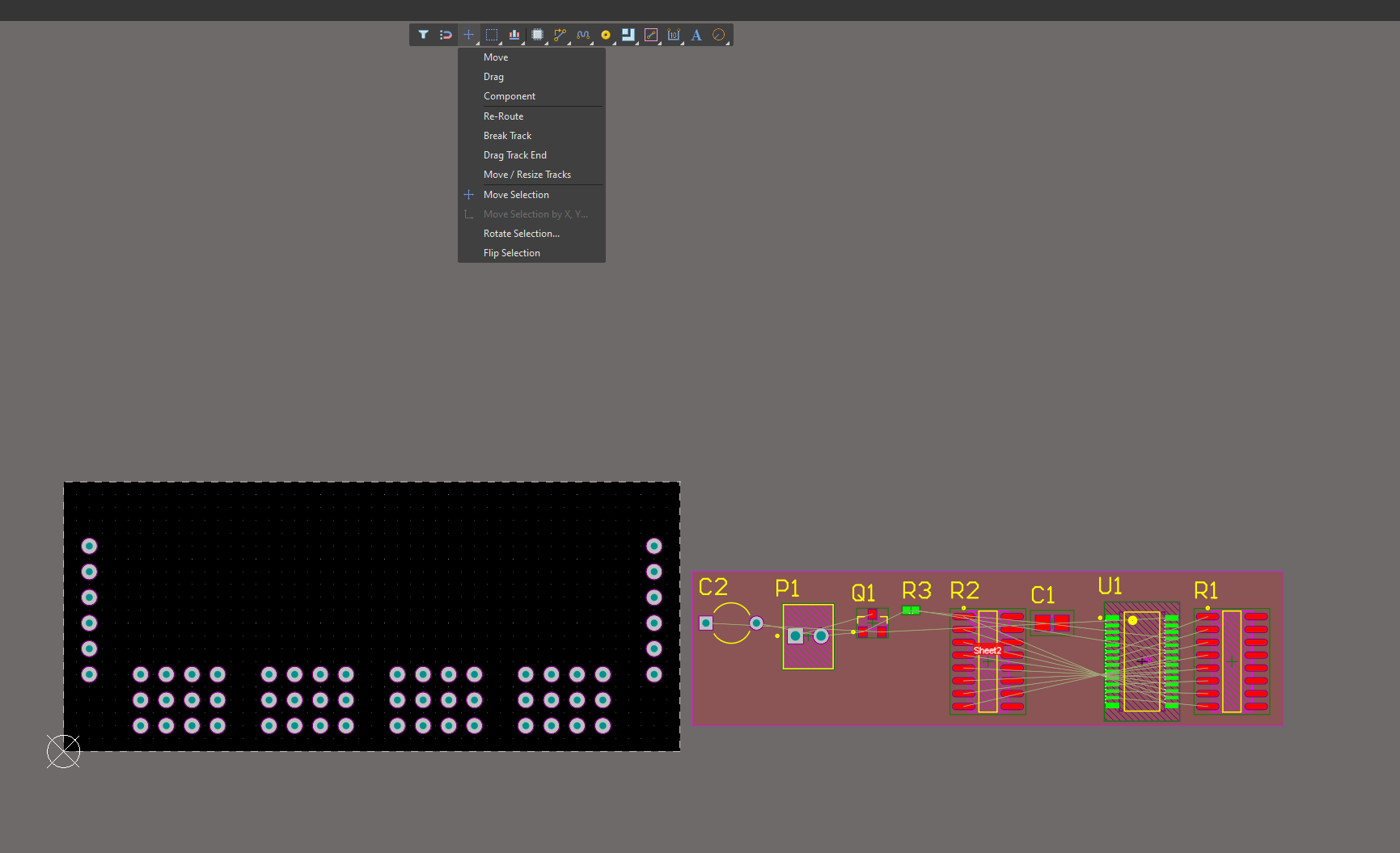
So, let's say, my main board here U1, I can just click and drag my board and bring it over to my actual board shape. Now, notice here, it's kind of jumping around into some strange angles, and that's because it's placing on my polar grid. So, for some, maybe, more complex board designs I may need to jump back and forth between grids. So, again, I'll navigate to my panels, my property panel, and just take a look at my grids here. So, let's say I want to go back to a Cartesian grid or just my default grids. So I'm just going to turn off my polar grid here for a second, so now I'm back to a more rectangular grid and I can again click and drag my U1 and now, I can say, I can place it and it's not going on those polar angles, there.
So let's say I place my U1 somewhere in the middle here, and then, it's a similar idea really for all of my components. Let's grab, maybe, JP2 here, and I'm going to click that and drag this guy here as well, and place it, maybe, somewhere about here. But, notice, here I can use my navigation tools of course. But I also have a couple other hot keys as well. So, again, my space bar will rotate my components by 90 degrees, just, very similar to how it did in the schematics, and I can also change which layer the component's on just by clicking the L key. L for Layer.
So we can see that's changing in the properties there, as well, from my top layer which is showing in red, to my bottom layer which is showing in blue. In this case, maybe I'll just keep it on the top layer for now. So, it's the L key to easily swap layers while placing components Also notice that as I'm moving these components I have these kind of temporary lines coming in. That's what we'll call a Rat's Nest, but essentially that's just showing where my electrical components are being connected. So, you'll want to use your Rat's Nest to kind of help with your placement, as you'll want those to be kind of as organized as possible, and that will just help with routing, the way it runs, you don't just have a mess of routes all over the places. They're a little bit more organized based on these Rat's Nest lines. So I'll place them right about here. Then, once, say I'm happy with that now maybe I want to start to place some other components on the polar grid. So, I can turn my polar grid back on, here and now let's see, click and drag some other components here (clicking) and now we can see that those are being placed, somewhere, say on my polar grid, and now again, hitting space. See, it still rotates ninety degrees, but it's now at that specific angle of my polar grid. So, let's say, place maybe a connection point about here, (clicking) here, and so on. I'm just running through this fairly quickly, and so on there. Okay, so you can see I've just very quickly just placed a few components on my board, here. I'm not going to go through the entire process, but the idea is, you want to have placed these in a way that will kind of make it most organized according to the Rat's Nest in your eventual routing.
# Design rule checks
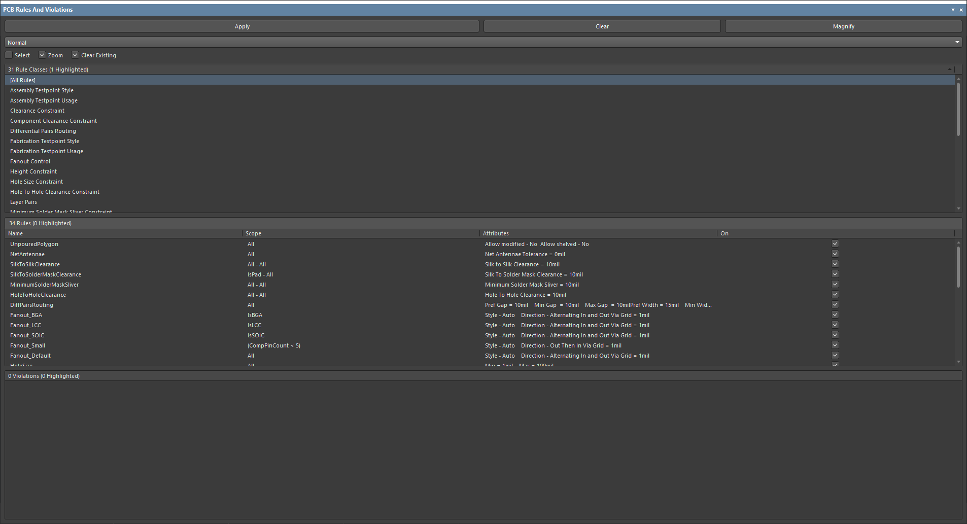
A critical aspect of PCB design is running through design rule of checks or essentially checking your designs or layouts for any potential issues or warnings or errors. So, thankfully Altium Designer helps me with this and its quite a simple process.
So I can just navigate down to my panels here and I'm going to turn on PBC rules and violations. So that's going to show me any current violations or warnings or errors within my PCB design here. Generally you'll run this near the end of a project but you're going to run it really all throughout a project as well to see any potential issues that there may be within your design. So we have a breakdown of all of the different rules here so it looks like I have 31 rules and I can go one by one through each of these and check my problems. Looks like I have some clearance constraints here. But I could also just click on all rules and that will run through all 31 and show me all my potential violations or issues. So it looks like I have a bunch of clearance constraints here and if I click on any of those, it does nice little highlight of those and also gives me a brief description here as well. So this is telling me that my two pads don't seem to have large enough clearance. Looks like it's about nine mil and my rule that has been set up is, be no less than 10 mil. So each of these are kind of giving me an error. So we have a number of errors there. Now looks like we also have one silk to silk clearance issue so let's take a look at that. And see so here we just see our silk to silk clearance issue for two components D4 and R2. This should be a simple fix and I can just fix it directly. I can just move a label here as an example. (clicking) Just going to move this D4 up a little bit and now notice that violation has automatically been removed. I only have 19 violations remaining. All clearance constraints. So there's a number of ways we can fix our violations, of course we can move things around, we can edit things, we can change, we can delete. But we also might need to alter our rules.
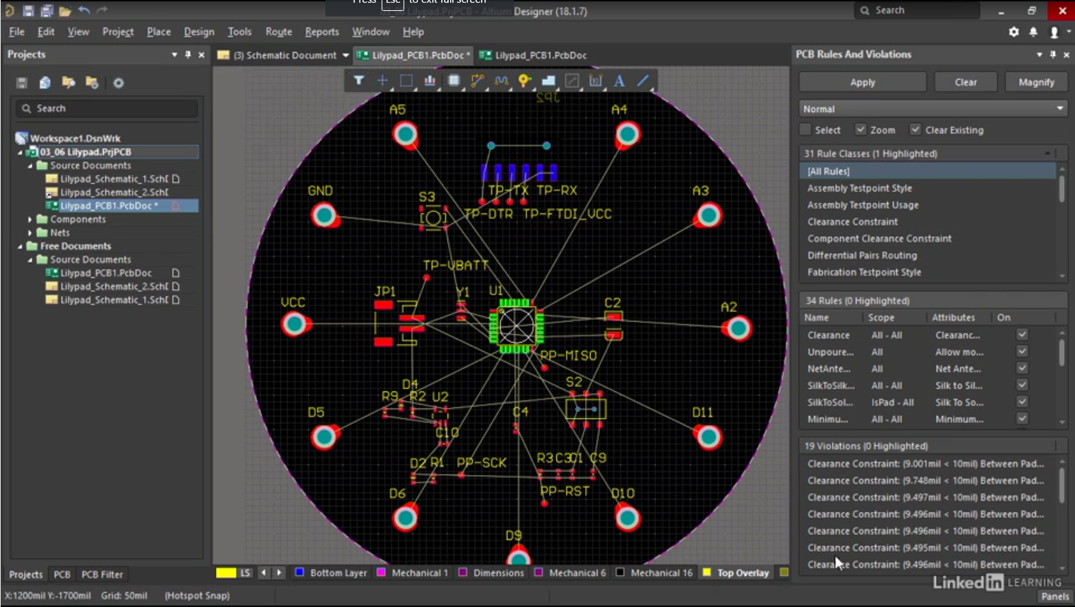
So where are these rules coming in? Where did I define that it must be at least 10 mil clearance thing? So let's take a look at this. And find these I can just go to designs and rules. So this shows me a list of all of my design rules. I can run through electrical rules, routing rules, clearance and so on. Manufacturing rules, a whole number of rules that I can set up and you're going to standardize these to your specific needs and specific projects. In this case, I know I had clearance problems so I'm going to jump into my clearance rule here and I'm seeing that my minimal, minimum clearance between traces and so on here and pads and everything all seems to be about 10 mil. So I can change that, alter that, maybe for my specific standards I actually don't need clearance of 10. Maybe I can change this to eight mil. And hit apply. Notice that applies to constraint clearances between a whole bunch of different components here. So now those have all been changed to my standard of eight mil. Say okay to that. And now if I went back to my potential violations, again, remember it was about nine mil clearance before. Now if I go to my PCB rules and violations, notice I see no violations so all of the kind of clearance issues that I was seeing with my U1 component there are now satisfied because I've changed my rule to be, instead of greater than 10 mil, I'm saying greater than eight mil.
# Routing the PCB layout
Once we have placed all of our components on our PCB board layout, we'll want to route them all up. them all up. So I can just navigate again to my active bar here and I have a few, a number of routing options. But the one you're most commonly going to use is most likely Interactive Routing here and then let's just take a quick look at routing up some components really quickly here. Pretty simple process I can just click once to start my route, kind of similar to wiring in the schematic, I notice I get a kind of a highlight of the pad that I'm on here, and then I want to follow that route to next line, to connect it up to my other component pad here. So I just click once to start, and route up to say here, and then I just repeat that process again, and again. Notice I have a number of routing options I can change here as well, so I'll start a route here and do something like this but say I want to change the general shape I can hit the ~ Tilde key and that will just pop up all of my kind of hotkeys for routing.
So for example if I wanted to toggle my Elbow Side I can just hit, button here, and notice that the hotkey for that is Space, Corner Style Shift + Space and so on. So let's try Toggle Elbow Style here and just notice how that changes things slightly and again if I remember that hotkey was space, so I can jump between Elbow Styles nice and quickly there. So again that was the Tilde key to jump to all of my hotkeys being shown, and just of course repeat this process to do essentially all of your routing here.
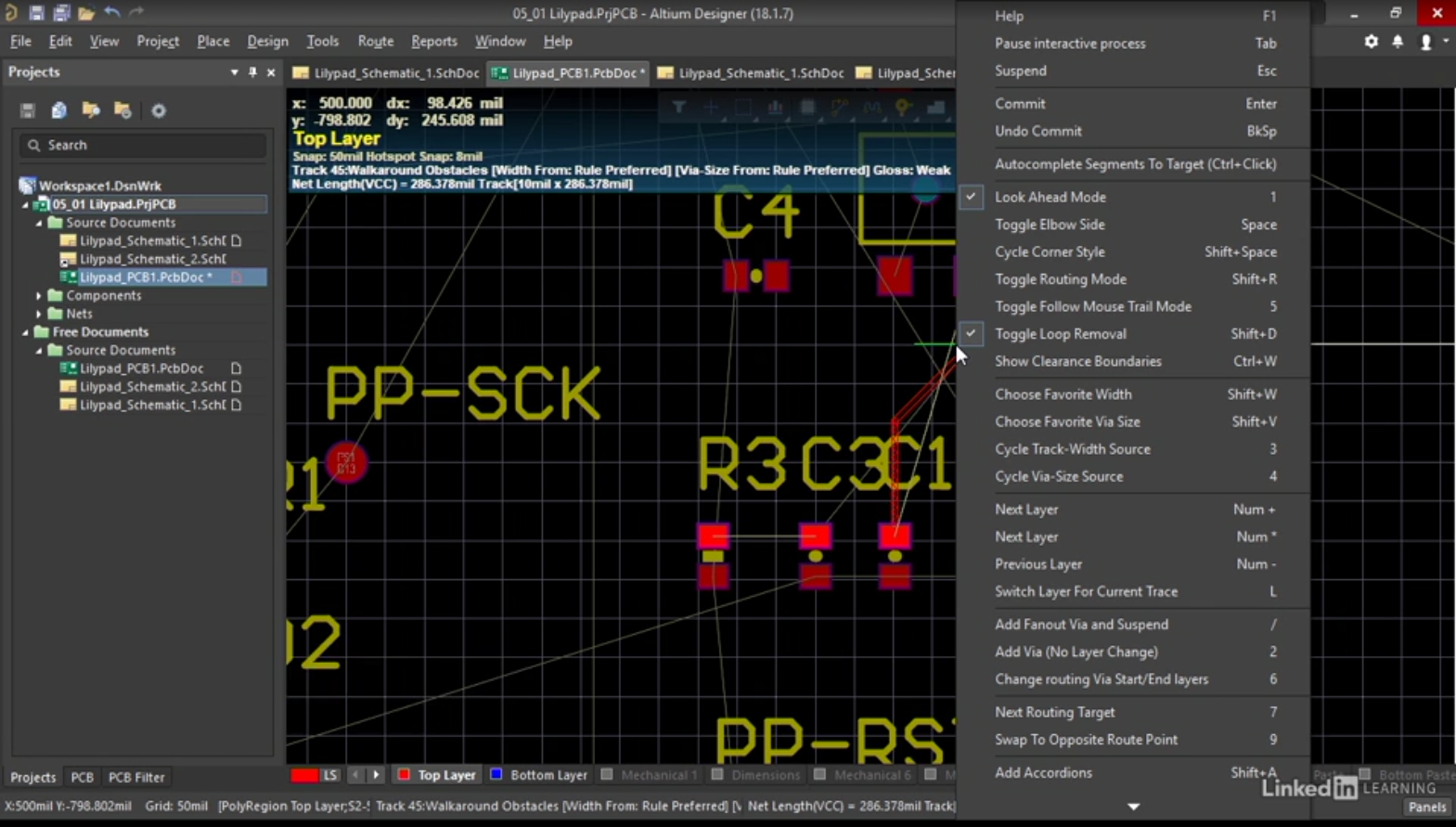
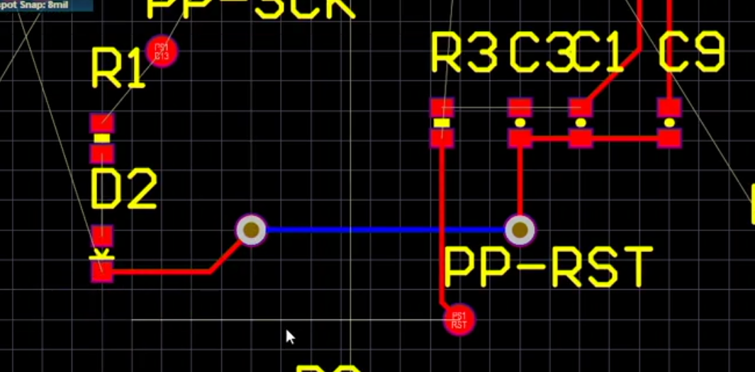
Now, another important aspect of routing is potentially using pads to jump through layers. So let's take a look at this, let's say I wanted to route this component pad here, over to my component D2 here, so there's a number of different ways, and this is obviously a fairly simple board design, so maybe I don't need too many paths to jump layers and so on but notice I can't of course, cross a signal or cross a trace here so I'd have to go over or around or up and over or whatever it might be. Which in this case I can do but in many cases you may need to jump layers, so for example if I could jump to my bottom layer and go underneath or above an existing trace. So to do that I can just go to let's say about here, and click plus and that will automatically add in a pad here, so let's say I click about here, let's say and notice what that does is it jumps me through to my other layer, my bottom layer in this case. But say I had a seven layer board, I could jump from layer to layer to layer in order to cross over traces here, and you can see that I'm in my bottom layer coming in the blue color there, I can click maybe somewhere about here and then plus again, at some point, because you know I want to get back to my top layer. So I can connect to my D2 component, and something like that to finish it off. So the idea being here is in order to cross this trace I had to throw in a couple of pads using the plus key, that just jumps me to the bottom layer so I can cross underneath my top layer, signal layer.
So essentially you just repeat all of these steps or processes until your PCB is fully routed. Now that being said, Altium Designer does give us a nice useful option for auto routing. This app will just take all the work out for us, and do it automatically for us, so to do that I can just go to route, dropdown, and I have Auto Route and I can Auto Route specific nets or specific classes and so on or I can just say Auto Route the entire board, all and I have a number of different routing strategies here in this case it's a two layer board so I'm going to use default to two layer board. But you can customize these to fit your exact needs, so each of these have a whole bunch of different routing parameters such as the routing widths, the via styles you like, the clearance rules you like. But you can set these all up to fit your specific company or standard needs. I'm just going to use the Altium defaults here and just click route all. This might take a few seconds to a few minutes depending on the complexity of your board here but you can see just within a few seconds it has routed up my entire PCB board for me. I'm saving me quite a bit of time, now that being said of course you should take a look at this a lot of designers prefer to manually route, the Auto Route unfortunately isn't exactly optimized quite yet, yes it does come up with a great solution, but maybe not the best or most clean or most organized routes and a lot of designers still of course prefer to manually route their boards.